Researchers at Harvard University in the United States have developed a platform to manipulate and understand silicon defects for quantum communications using existing telecommunications infrastructure.
From Harvard John A. Paulson School of Engineering and Applied Sciences 25/06/24.
The quantum internet would be a lot easier to build if we could use existing telecommunications technologies and infrastructure.
Over the past few years, researchers have discovered defects in silicon — a ubiquitous semiconductor material — that could be used to send and store quantum information over widely-used telecommunications wavelengths.
Could these defects in silicon be the best choice among all the promising candidates to host qubits for quantum communications?
“It’s still a Wild West out there,” said Evelyn Hu, the Tarr-Coyne Professor of Applied Physics and of Electrical Engineering at the Harvard John A. Paulson School of Engineering and Applied Sciences (SEAS).
“Even though new candidate defects are a promising quantum memory platform, there is often almost nothing known about why certain recipes are used to create them, and how you can rapidly characterize them and their interactions, even in ensembles.”
“And ultimately, how can we fine-tune their behavior so they exhibit identical characteristics?”
“If we are ever to make a technology out of this wide world of possibilities, we must have ways to characterize them better, faster and more efficiently.”
Now, Hu and a team of researchers have developed a platform to probe, interact with and control these potentially powerful quantum systems.
The device uses a simple electric diode, one of the most common components in semiconductor chips, to manipulate qubits inside a commercial silicon wafer.
Using this device, the researchers were able to explore how the defect responds to changes in the electric field, tune its wavelength within the telecommunications band and even turn it on and off.
“One of the most exciting things about having these defects in silicon is that you can use well-understood devices like diodes in this familiar material to understand a whole new quantum system and do something new with it,” said Aaron Day, a Ph.D. candidate at SEAS.
Day co-led the work with Madison Sutula, a research fellow at Harvard.
While the research team used this approach to characterize defects in silicon, it could be used as a diagnostic and control tool for defects in other material systems.
The research is published in Nature Communications.
Quantum defects, also known as colour centres or quantum emitters, are imperfections in otherwise perfect crystal lattices that can trap single electrons.
When those electrons are hit with a laser, they emit photons in specific wavelengths.
The defects in silicon that researchers are most interested in for quantum communications are known as G-centres and T-centres.
When these defects trap electrons, the electrons emit photons in a wavelength called the O-band, which is widely used in telecommunications.
In this research, the team focused on G-centre defects.
The first thing they needed to figure out was how to make them.
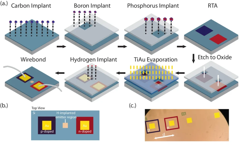
Unlike other types of defects, in which an atom is removed from a crystal lattice, G-centre defects are made by adding atoms to the lattice, specifically carbon.
But Hu, Day and the rest of the research team found that adding hydrogen atoms is also critical to consistently forming the defect.
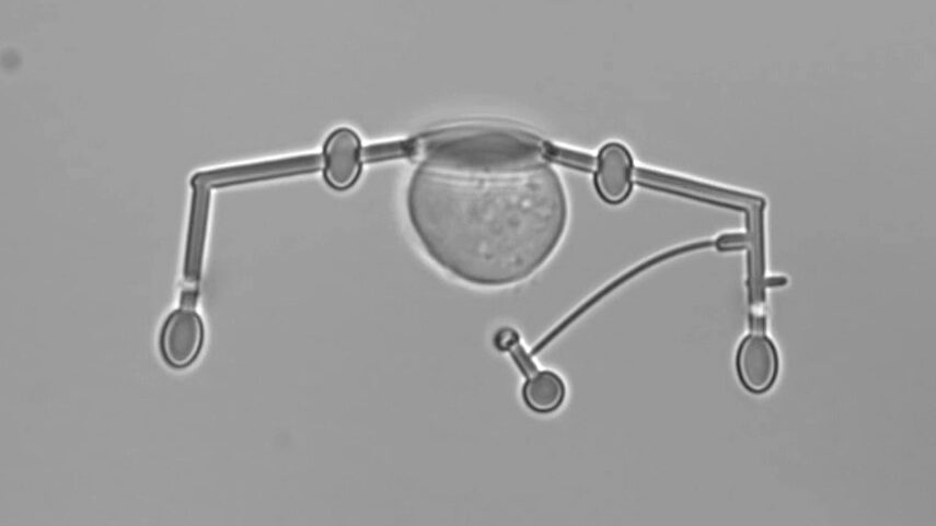
Next, the researchers fabricated electrical diodes using a new approach which optimally sandwiches the defect at the centre of every device without degrading the performance of either the defect or the diode.
The fabrication method can create hundreds of devices with embedded defects across a commercial wafer.
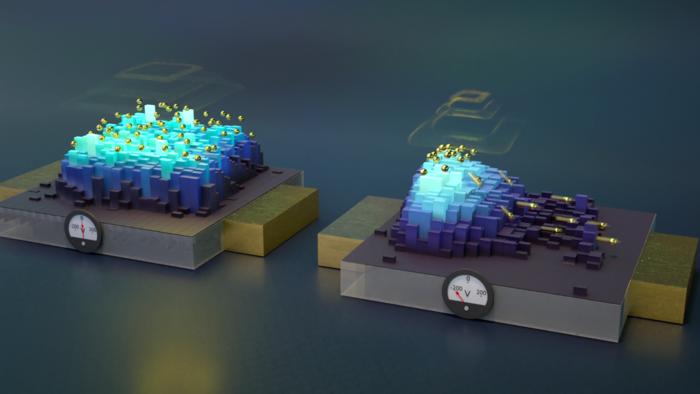
Hooking the whole device up to apply a voltage, or electric field, the team found that when a negative voltage was applied across the device, the defects turned off and went dark.

“Understanding when a change in environment leads to a loss of signal is important for engineering stable systems in networking applications,” said Day.
The researchers also found that by using a local electric field, they could tune the wavelengths being emitted by the defect, which is important for quantum networking when disparate quantum systems need to be aligned.
The team also developed a diagnostic tool to image how the millions of defects embedded in the device change in space as the electric field is applied.
“We found that the way we’re modifying the electric environment for the defects has a spatial profile, and we can image it directly by seeing the changes in the intensity of light being emitted by the defects,” said Day.
“By using so many emitters and getting statistics on their performance, we now have a good understanding of how defects respond to changes in their environment.”
“We can use that information to inform how to build the best environments for these defects in future devices.”
“We have a better understanding of what makes these defects happy and unhappy.”
Next, the team aims to use the same techniques to understand the T-centre defects in silicon.
The research was co-authored by Sutula, Jonathan R. Dietz, Alexander Raun from SEAS, and AWS research scientists Denis D. Sukachev and Mihir K. Bhaskar.
This work was supported by AWS Center for Quantum Networking and the Harvard Quantum Initiative.
Harvard’s Office of Technology Development has protected the intellectual property associated with this project and is pursuing commercialisation opportunities.