From University of Sydney 03/12/23
Researchers at the University of Sydney Nano Institute have invented a compact silicon semiconductor chip that integrates electronics with photonic, or light, components.
The new technology significantly expands radio-frequency (RF) bandwidth and the ability to accurately control information flowing through the unit.
Expanded bandwidth means more information can flow through the chip.
The inclusion of photonics allows for advanced filter controls, creating a versatile new semiconductor device.
Researchers expect the chip will have application in advanced radar, satellite systems, wireless networks.
The chip is also anticipated to be significant in the roll-out of 6G and 7G telecommunications.
It could open the door to advanced sovereign manufacturing.
It could also assist in the creation of high-tech value-add factories at places like Western Sydney’s Aerotropolis precinct.
The chip is built using an emerging technology in silicon photonics.
This technology allows integration of diverse systems on semiconductors less than 5 millimetres wide.
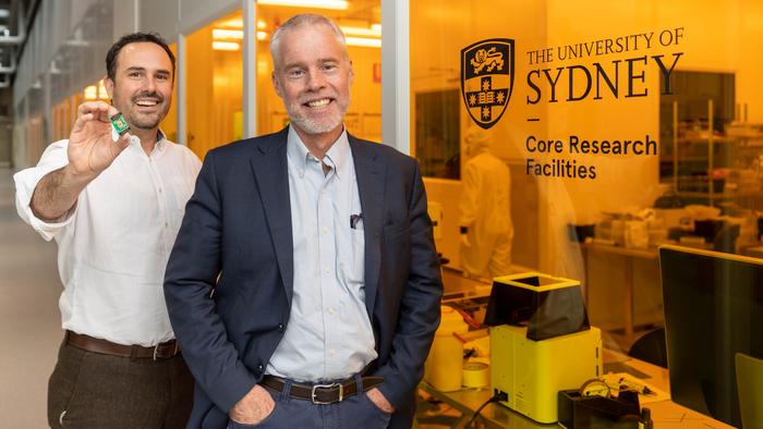
Pro-Vice-Chancellor (Research) Professor Ben Eggleton, who guides the research team, likened it to fitting together Lego building blocks.
New materials are integrated through advanced packaging of components, using electronic ‘chiplets’.
The research for this invention has been published in Nature Communications.
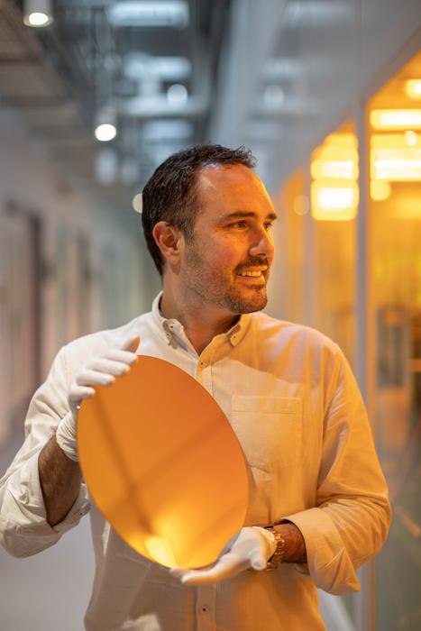
Dr Alvaro Casas Bedoya, Associate Director for Photonic Integration in the School of Physics, led the chip design.
He said the unique method of heterogenous materials integration has been 10 years in the making.
“The combined use of overseas semiconductor foundries to make the basic chip wafer with local research infrastructure and manufacturing has been vital in developing this photonic integrated circuit,” he said.
“This architecture means Australia could develop its own sovereign chip manufacturing without exclusively relying on international foundries for the value-add process.”
Professor Eggleton highlighted the importance of semiconductors in critical technologies.
He said the invention aligns with initiatives like the Semiconductor Sector Service Bureau (S3B), sponsored by the NSW Government.
Dr Nadia Court, Director of S3B, commented on the significance of this work for semiconductor innovation in Australia.
The integrated circuit was designed in collaboration with scientists at the Australian National University.
It was built at the Core Research Facility cleanroom at the University of Sydney Nanoscience Hub.
The photonic circuit in the chip enables a device with a 15 gigahertz bandwidth of tunable frequencies.
The spectral resolution is down to just 37 megahertz, which is less than a quarter of one percent of the total bandwidth.
Professor Eggleton described this invention as a significant advance for microwave photonics and integrated photonics research.
“Our innovative approach of integrating advanced functionalities into semiconductor chips, particularly the heterogenous integration of chalcogenide glass with silicon, holds the potential to reshape the local semiconductor landscape.”


References:
Cherokee casino siloam springs https://amberjgbb807873.qowap.com/100606819/casino-of-gold-dein-ultimativer-guide
References:
Online Casino Eckental GTA 5 Casino Karte
References:
Legiano Casino Anmeldung https://jpn1.fukugan.com/
References:
Hampton casino https://metager.de/meta/settings?fokus=web&url=http://www.sinp.msu.ru/ru/ext_link?url=https://de.trustpilot.com/review/owowear.de
References:
Legiano Casino Sicherheit http://www.smartphone.ua/buy/?f=1&s=105&u=http://voffice.lawyers.bh/yhcclara64186
References:
Legiano Casino Gutscheincode https://forums.eq2wire.com/proxy.php?link=https://k1t.kr/rafaelar188354
References:
Legiano Casino Video Review http://www.visit-x.net
References:
Legiano Casino Bonus Code https://bios-fix.com
References:
KingMaker echtgeld einzahlung mydaradstools.com
References:
Kingmaker casino apple pay einzahlung https://unim.ma/eeujulianne52
References:
KingMaker Casino Ersteinzahlungsbonus https://link.mym.ge/hjfjason584303
References:
KingMaker einzahlung sofortüberweisung mylinkbox.me
References:
KingMaker Casino Einzahlungsbonus ohne Umsatzbedingungen zooshans.by
References:
Kingmaker Casino Freispiele http://toolbarqueries.google.com.nf
References:
KingMaker einzahlung apple pay http://ads1.opensubtitles.org
References:
Legiano Casino Download http://maps.google.com.br/url?q=https://bridgedesign.space/wiki/Legiano_Casino_Test_2026_Ist_es_seris
References:
Legiano Casino Mindestauszahlung https://perevodvsem.ru
References:
Legiano Casino Web App images.google.com.ua
References:
Hitnspin casino bewertung images.google.com.ph
References:
Hitnspin erfahrungen sites.fastspring.com
References:
Hitnspin registrierung https://nexus.astroempires.com/redirect.aspx?https://link.zhihu.com/?target=https://de.trustpilot.com/review/der-wikinger-shop.dehttps://nexus.astroempires.com/redirect.aspx?https://link.zhihu.com/?target=https://de.trustpilot.com/review/der-wikinger-shop.de</a
References:
Hit n spin promo code cse.google.ki
References:
Hitnspin bonus code douban.com
References:
Hitnspin casino betrug https://link.avito.ru/
References:
Hitnspin casino bonus curiouscat.net
References:
Hitnspin promo code http://www.proplay.ru/redirect/www.news.lafontana.edu.co/profile/padillaqynennis89233/profile
References:
Hitnspin gutscheincode https://astrakhanica-personalia.ru
References:
Hit n spin casino online login http://remit.scripts.mit.edu/trac/search?q=https://www.news.lafontana.edu.co/profile/thorhaugeppclodberg74346/profile
References:
Monro Casino Bonus Code http://gamer.kg/proxy.php?link=https://avido.by/bitrix/click.php?goto=https://de.trustpilot.com/review/deincorazon.de
References:
Lollybet Casino mit Echtgeld http://cse.google.com.ni/url?sa=i&url=http://videos.awaregift.com/@milagrosbrouss?page=about
References:
Lollybet Casino No Deposit Bonus http://maps.google.ro/url?sa=t&url=https://rifleknife0.bravejournal.net/deine-online-spielothek
References:
Lollybet Casino Bonus https://blackmod.net/dl/?url=aHR0cHM6Ly91bmRydG9uZS5jb20vcXVhaWxsaW1pdDg
References:
Lollybet Casino Mobile http://images.google.co.il/url?sa=t&url=http://videos.awaregift.com/@milagrosbrouss?page=about
References:
Lollybet Casino mit Echtgeld http://toolbarqueries.google.kz
References:
Lollybet Casino No Deposit http://image.google.me/
References:
Hitnspin casino auszahlung erfahrungen http://clients1.google.co.cr/
References:
Hitnspin casino auszahlungsdauer clients1.google.com.sa
References:
Hitnspin casino ähnliche casinos clients1.google.com.mx
References:
Hitnspin casino kundenbewertungen http://maps.google.is
References:
Hitnspin casino bonuscode http://coinsplanet.ru
References:
Hit’n’spin casino 50 free spins http://chat.chat.ru/redirectwarn?http://support.roombird.ru/index.php?qa=user&qa_1=robinfarmer69
References:
Payid online pokies https://git.ddns.net/
References:
Online pokies with payid https://healthjobslounge.com/
References:
Instant payid pokies australia https://git.solutionsinc.co.uk/
References:
Online pokies real money payid https://gladjobs.com
References:
Lollybet Casino Neukundenbonus http://alt1.toolbarqueries.google.vg/
References:
Lollybet Online Casino https://psychopathfree.com/
References:
Lollybet Casino Neukundenbonus wiki.fd.io
References:
Lollybet Casino Willkommensbonus https://60.cholteth.com/
References:
Lollybet Casino Bitcoin toolbarqueries.google.cl
References:
Lollybet Casino http://images.google.ie
References:
Lollybet Bewertung images.google.cg
References:
Lollybet Casino Download www32.ownskin.com
References:
Lollybet Casino Lizenz xxx-files.org